Intel 18A-P vs TSMC A16 The VLSI Showdown in Advanced Process Nodes
5/7/2026 10:19:16 PM
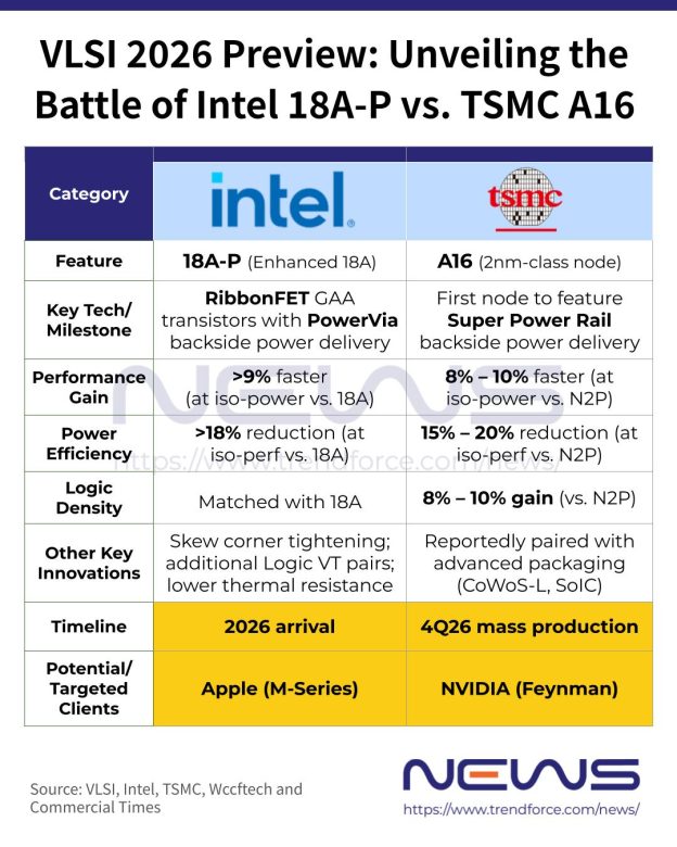
Industry rumors suggest Apple is poised to become an early adopter of Intel's 18A-P process, applying it to future M-series chips, with more technical details expected to be unveiled at the VLSI Symposium in mid-June. According to the VLSI website, compared to the standard 18A process, Intel's upgraded 18A-P reduces power consumption by over 18% at the same performance, or boosts performance by over 9% at the same power.
Against this backdrop, the upcoming VLSI Symposium has become a critical battleground for the advanced process competition between Intel and TSMC. It is reported that TSMC will unveil its 2nm-class A16 Angstrom CMOS technology at the event, which adopts Gate-All-Around (GAA) transistors and features a new "Super Power Rail" (SPR) design for backside power delivery.
Intel has pre-released some core details of the 18A-P process. According to media reports, 18A-P's key structural parameters (including cell height and contacted poly pitch) remain consistent with the base 18A process. The upgrades focus on transistor-level tuning and voltage optimization: the number of threshold voltage (VT) BT options has expanded from 4 in 18A to over 5 in 18A-P, with the addition of a new logic VT option between Ultra-Low VT and Low VT.
Furthermore, the 18A-P process enhances process variability control and thermal efficiency, providing critical support for its low-power, high-performance profile. This is a key reason for the increased interest from Apple and other fabless chip designers. To achieve these gains, Intel introduced new variants of its RibbonFET GAA transistors, including enhanced-contact high-performance transistors and optimized low-power devices, solidifying the foundation for the improvements.
Notably, Intel revealed it has tightened the skew corners by 30% in the 18A-P process, thereby improving performance consistency and reducing variability. Skew corners refer to the differences in transistor performance and power characteristics across a process node; as semiconductor processes advance, transistor behavior becomes increasingly non-uniform, making variability control paramount.
Intel's first product based on the 18A process, Panther Lake, entered mass production at the end of 2025. Its 18A-derived processes will be rolled out in phases: 18A-P is expected to land in 2026, with a further upgraded 18A-PT planned for 2028.
Meanwhile, TSMC is preparing for the debut of its A16 process. As its first node based on the Super Power Rail, A16 is scheduled for official release at the VLSI Symposium from June 14–18. According to TSMC, compared to the performance-enhanced N2P node, A16 offers an 8–10% performance gain at the same power, or a 15–20% power reduction at the same performance, along with an additional 8–10% logic density improvement.
TSMC plans to achieve mass production of the A16 process in the fourth quarter of 2026. Industry rumors widely suggest that NVIDIA's Feynman chip will be the first product to adopt it. Supply chain information indicates that A16 will be paired with CoWoS-L and SoIC advanced packaging technologies, enabling system scaling up to 9.5x the reticle size, primarily targeting high-performance computing (HPC) workloads.
Related information


- One-stop procurement solution

- Cost down and save your time

- Reliable package and fast delivery

- 365 days after-sales service and warranty